Flexible designs, high throughput, uniformity, and yield are the basic requirements in the semiconductor industry. The MLA 300 Maskless Aligner meets all of these requirements.
1 – 10 – 100 – 1000.
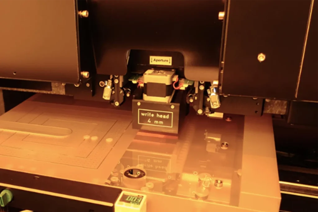
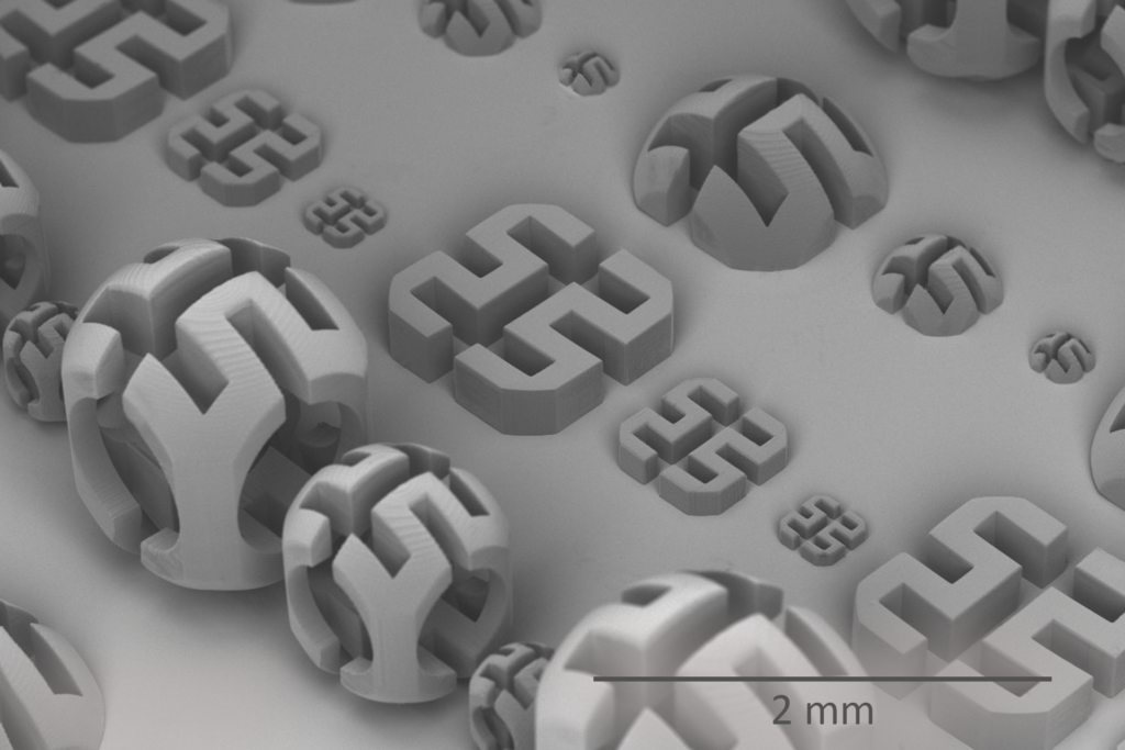
The MPO 100 is a Two-Photon Polymerization (TPP) Multi-User Tool for 3D Lithography and 3D Microprinting of microstructures with applications in optics, photonics, mechanics, and biomedical engineering.
Heidelberg Instruments - The Power of direct writing
Heidelberg Instruments is a world leader in the design, development, and manufacture of high-precision laser lithography systems, maskless aligners, and nanofabrication tools.
With 40 years of experience and well over 1,400 systems installed worldwide, Heidelberg Instruments provides lithography solutions specifically tailored to meet the micro- and nanofabrication requirements of our global customers – no matter how challenging. In our Process and Application Labs (PAL) located in Germany, Switzerland, and China, the engineers train and collaborate closely with our customers to make the most of their Heidelberg Instruments equipment.
Industry stakeholders, as well as working groups of the most renowned universities and research institutes all over the world, use Heidelberg Instruments’ systems for advanced micro- and nanopatterning. Fields of application are in micro-optics and microsystems technology, photonics, electronics, semiconductors/advanced packaging, quantum computing, MEMS/NEMS, micro-mechanics, biomedical engineering, 2D materials, IoT, and many more.
Applications | Technologies | Key Features
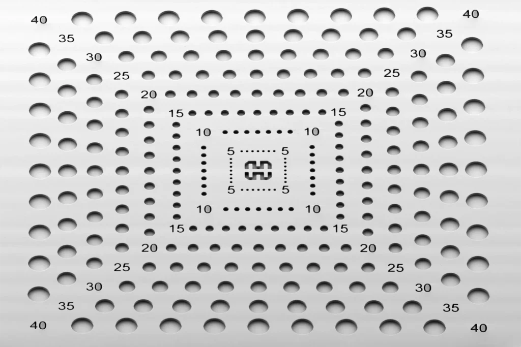
Applications
Products
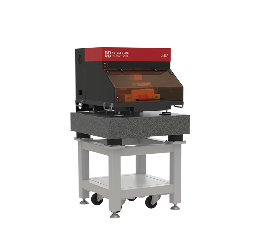
µMLA
- Maskless Aligner
Configurable and compact tabletop maskless aligner with raster scan and vector exposure modules.
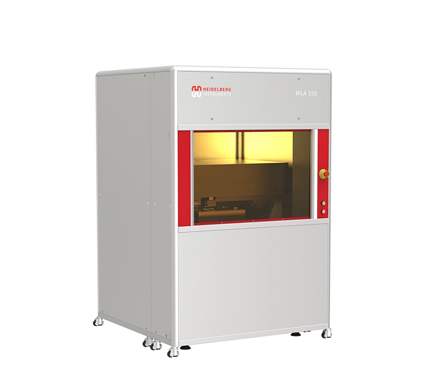
MLA 150
- Maskless Aligner
The fastest maskless tool for rapid prototyping, the alternative to the mask aligners. Perfect for standard binary lithography.
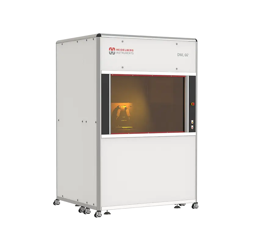
DWL 66+
- Direct Write Laser Lithography System
Our most versatile system for research and prototyping with variable resolution and wide selection of options.
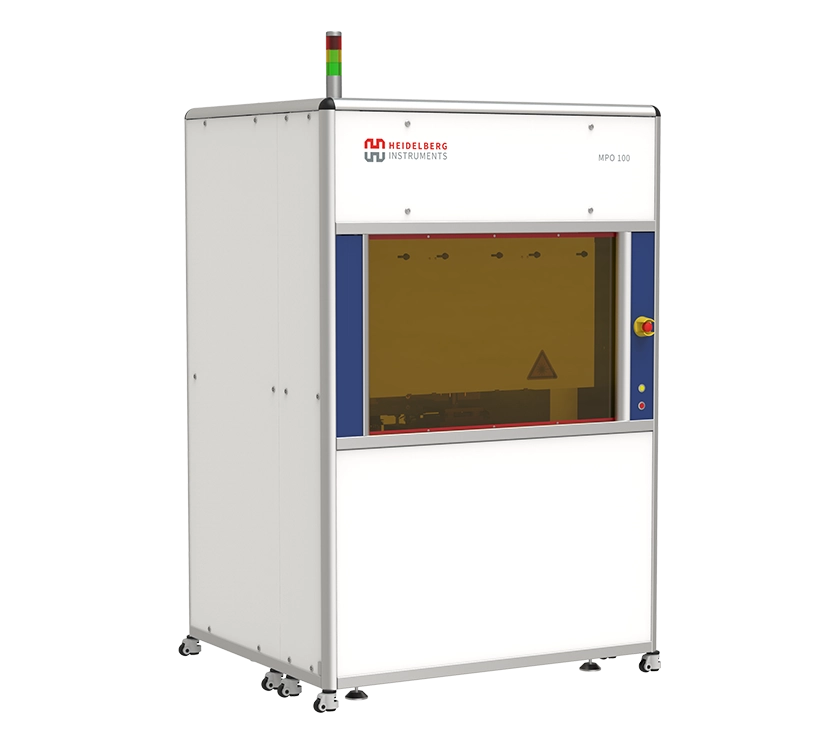
MPO 100
- Two-Photon Polymerization Multi-User Tool
Multi-User Tool for 3D Lithography and 3D Microprinting of microstructures with applications in micro-optics, photonics, micro-mechanics and biomedical engineering.
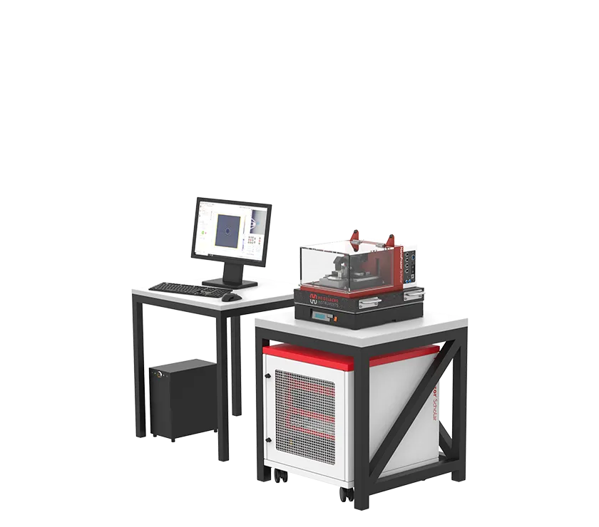
NanoFrazor Scholar
- Thermal Scanning Probe Lithography System
Table-top thermal scanning probe lithography system with in-situ AFM imaging. Compact and compatible with glovebox.
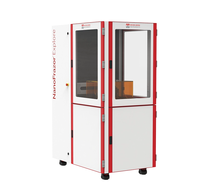
NanoFrazor Explore
- Thermal Scanning Probe Lithography System
Thermal scanning probe lithography tool with direct laser sublimation and grayscale modules. Excellent alternative to e-beam lithography tools.
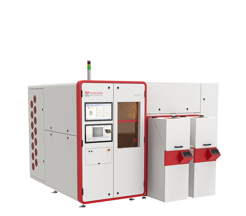
MLA 300
- Maskless Aligner
Optimized for industrial production with highest throughput and seamless integration into industrial production lines.
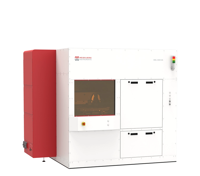
DWL 2000 GS / DWL 4000 GS
- Direct Write Laser Lithography System
The most advanced industrial grayscale lithography tool on the market.
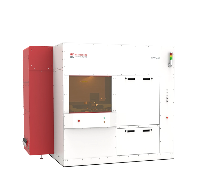
VPG+ 200 / VPG+ 400
- Volume Pattern Generator
A production tool for standard photomasks and microstructures in i-line resists.
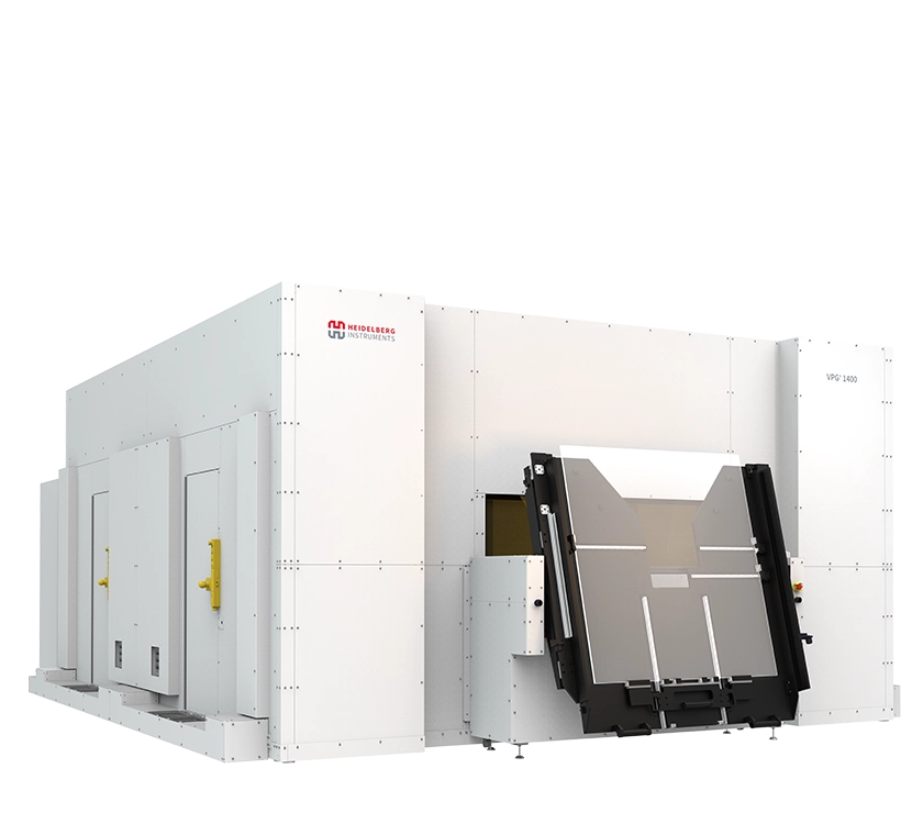
VPG+ 800 / VPG+ 1400
- Volume Pattern Generator
Photomask production on large substrates, perfect for display applications.

VPG 300 DI
- Maskless Stepper
Maskless direct imager for high-accuracy and high-resolution microstructures.
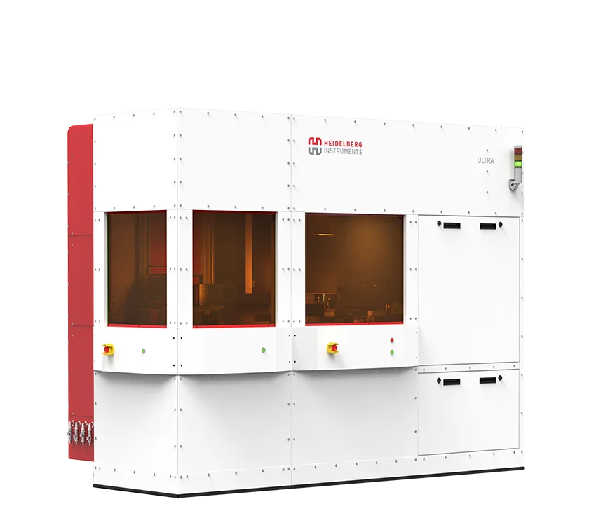
ULTRA
- Laser Mask Writer
A tool specifically designed to produce mature semiconductor photomasks.
Newsblog
MPO 100 successfully installed at Kyoto University
Exciting news! At Kyoto University Nanotechnology Hub one MPO 100 3D microprinting system and one MLA 150 maskless lithography system have been successfully installed. This Nanotechnology Hub is an open
Thermal Probe Workshop 2024 – Thank You for a Successful Event
A look back on the 8th Thermal Probe Workshop We were delighted to host a community of nanotechnology experts, fabrication researchers, rising stars and innovative leaders from all over the
Combining one- and multiphoton direct laser writing
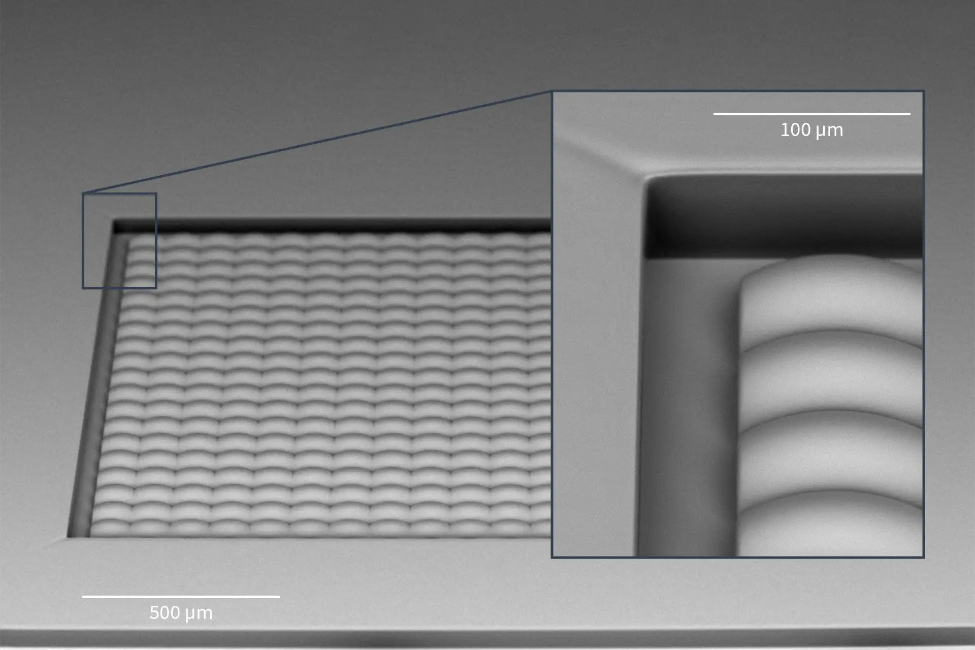
Achieve high throughput and resolution. Despite its unique capacity for three-dimensional fabrication with minimal feature sizes below 100 nm, achieving high throughput with Two-Photon Polymerization (TPP) remains a challenge, when
Would you like to know more about our system portfolio, key features, our corresponding core technologies or possible applications?
Meet us at exhibitions and conferences year-round.
Dates | Events
Photomask Japan 2024
Annex Hall, Pacifico Yokohama | Yokohama, Japan
MEMS Engineer Forum (MEF) 2024
KFC Hall Ryogoku | Tokyo, Japan
mAm 2024 – Micronarc Alpine Meeting
Hotel Viu | Villars-sur-Ollon, Switzerland
2024 E-MRS Spring Meeting
Strasbourg Convention and Exhibition Centre | Strasbourg, France
About us
From diverse culture and far-reaching history to forward-looking state-of-the-art scientific research facilities – Heidelberg has it all. A city with over 800 years of history and tradition is also home to numerous leading researchers and Nobel Prize winners. As a center for scientific research, Heidelberg not only houses prestigious universities and industrial research institutions but is also the home of Heidelberg Instruments Mikrotechnik GmbH.
Heidelberg Instruments was founded in 1984 by five scientists from various institutions in Heidelberg with the aim of building a high-tech company that transfers academic research and developments to industrial projects. In the past 35+ years it has become the core of innovation in the development of high-resolution microlithography pattern generators at Heidelberg Instruments.
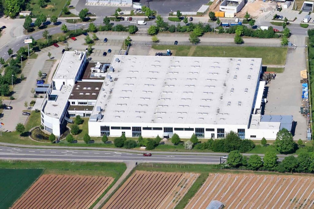
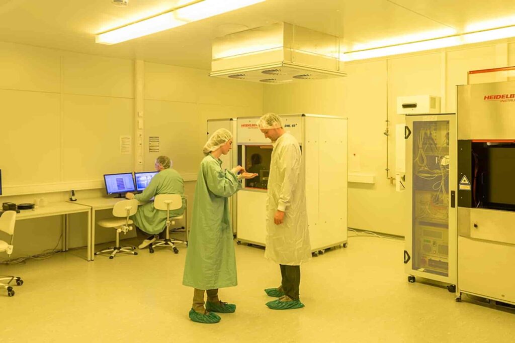
Heidelberg Instruments has evolved to become a world leader in the development and production of high-precision photolithography systems, maskless aligners, two-photon-polymerization lithography systems, and nanofabrication tools.
Individual commitment and excellent teamwork – two opposites that have been and continue to be essential for successfully growing our business for the past 35+ years. Together we innovate solutions, develop improvements, and contribute to the constant growth of Heidelberg Instruments.
Would you like to become a part of our growing team? Learn more about careers and available positions at Heidelberg Instruments.
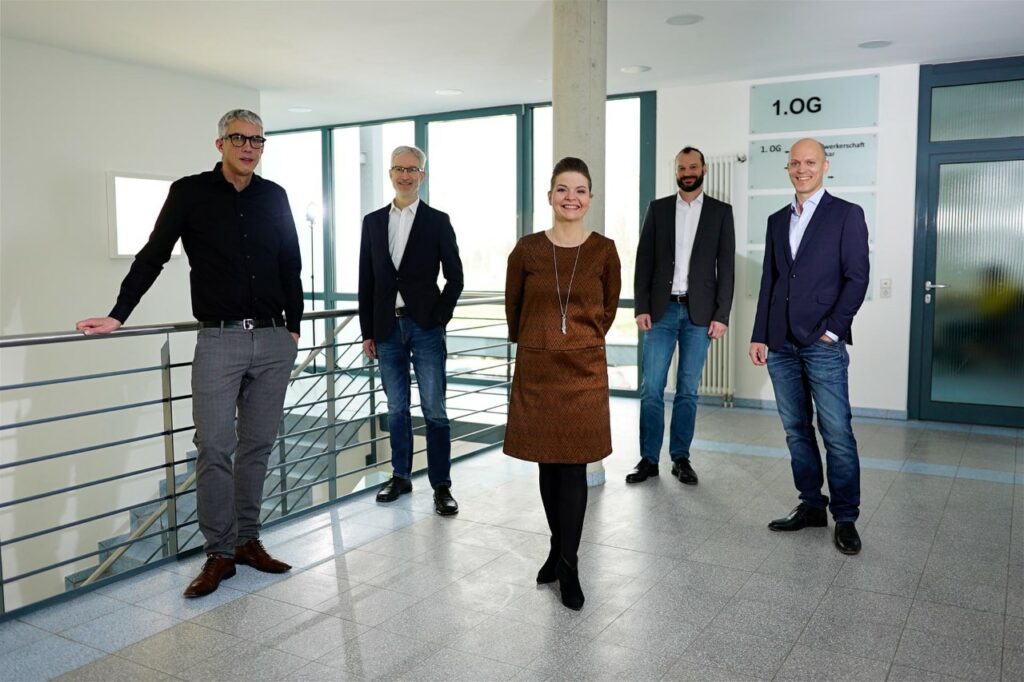
Our executive team consists of industry experts with decades of market experience. Together they ensure our operations run smoothly and efficiently, all while keeping the interest of our customers at the forefront. Their long-standing affiliation Heidelberg Instruments provides a firm sense of stability to both our clients and staff.
Heidelberg Instruments started in Heidelberg, Germany and has expanded its reach with subsidiary offices to seven different countries, including the US and China, to serve our global customer base and interested parties.
Additionally, global partner offices represent our products, applications and technologies in other countries without subsidiary coverage.
